
Semiconductor manufacturing equipment consists of specialized machines used to produce, process, inspect, assemble, and test semiconductor devices.
As electronic devices become smaller and more powerful, semiconductor production requires advanced equipment capable of controlling materials at extremely small scales. These technologies support computing, telecommunications, automotive electronics, artificial intelligence, medical devices, and industrial automation.
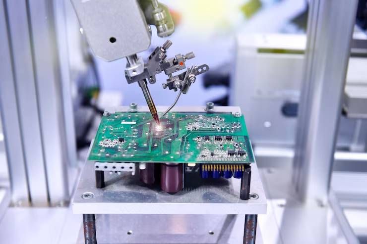
1. Understanding Semiconductor Manufacturing Equipment
Semiconductor manufacturing equipment refers to specialized machinery used to manufacture semiconductor devices from silicon wafers and other semiconductor materials. The equipment operates in controlled environments to minimize contamination and maintain precise manufacturing conditions.
A semiconductor fabrication facility, commonly called a fab, contains multiple equipment categories. Each category performs a specific operation within a complex production sequence.
Major equipment functions include:
Preparing and processing semiconductor wafers
Transferring circuit patterns onto wafer surfaces
Depositing thin films of specialized materials
Removing selected material through etching
Modifying electrical properties through doping
Cleaning wafers between manufacturing stages
Inspecting microscopic structures and detecting defects
Testing finished semiconductor devices
The equipment required depends on the semiconductor technology, wafer diameter, device architecture, production volume, and required performance characteristics.
2. Major Types of Semiconductor Manufacturing Equipment
2.1 Wafer Processing Equipment
Wafer processing equipment prepares and modifies semiconductor wafers throughout fabrication. Silicon wafers are widely used because their electrical properties can be precisely controlled.
Common wafer processing operations include surface preparation, oxidation, polishing, cleaning, and thermal treatment.
Wafer cleaning systems remove particles, chemical residues, and contaminants that could affect circuit performance. Chemical mechanical planarization equipment creates smoother surfaces by combining chemical reactions with mechanical polishing.
2.2 Photolithography Equipment
Photolithography equipment transfers circuit patterns onto a wafer using light-sensitive materials called photoresists.
The process generally involves coating a wafer with photoresist, exposing selected areas through a patterned mask or reticle, developing the pattern, and preparing the wafer for subsequent processing.
Major equipment includes:
Deep ultraviolet (DUV) lithography systems
Extreme ultraviolet (EUV) lithography systems
Photoresist coating and developing tracks
Mask and reticle handling equipment
Alignment and overlay measurement systems
EUV lithography supports the production of advanced semiconductor structures with extremely small features. DUV systems remain widely used for many device layers and semiconductor manufacturing technologies.
2.3 Thin-Film Deposition Equipment
Deposition equipment forms thin layers of materials on semiconductor wafers. These layers may act as conductors, insulators, barriers, or semiconductor structures.
Common deposition technologies include:
Chemical Vapor Deposition (CVD): Uses chemical reactions to form thin films on wafer surfaces.
Physical Vapor Deposition (PVD): Deposits material through physical processes, such as sputtering.
Atomic Layer Deposition (ALD): Builds thin films through controlled, sequential surface reactions.
Epitaxial Deposition: Grows crystalline material with a defined relationship to the underlying substrate.
Deposition technologies are selected according to film thickness, uniformity, composition, electrical properties, and device design.
2.4 Etching Equipment
Etching systems selectively remove material to create circuit patterns and device structures.
Two major categories are wet etching and dry etching.
Wet etching uses liquid chemical solutions to dissolve selected materials. Dry etching typically uses plasma or reactive gases to remove material with greater directional control.
Plasma etching is important in advanced semiconductor fabrication because it enables the formation of narrow trenches, contact openings, and complex three-dimensional structures.
Etching performance depends on selectivity, uniformity, profile control, and the ability to minimize damage to surrounding materials.
2.5 Ion Implantation Equipment
Ion implantation equipment modifies the electrical properties of semiconductor materials by introducing controlled quantities of dopant atoms.
The process accelerates ions toward a wafer, allowing dopants to enter selected regions of the semiconductor. Subsequent thermal processing may activate the dopants and repair implantation-related crystal damage.
Ion implantation is used to form transistor regions, junctions, and other structures that control current flow within semiconductor devices.
2.6 Thermal Processing Equipment
Thermal processing equipment heats wafers under carefully controlled conditions to change material properties or complete chemical reactions.
Common systems include rapid thermal processing equipment, oxidation furnaces, diffusion furnaces, and specialized annealing systems.
These tools support dopant activation, film formation, material modification, and defect reduction. Temperature uniformity and process duration are important because excessive heat can affect device structures.
2.7 Chemical Mechanical Planarization Equipment
Chemical mechanical planarization (CMP) equipment removes material from wafer surfaces to create flat, uniform layers.
Planarization is necessary because repeated deposition and patterning can create uneven surfaces. Without sufficient flatness, subsequent lithography and processing operations may become less accurate.
CMP systems typically combine a polishing pad, slurry delivery, controlled pressure, wafer movement, and endpoint monitoring.
2.8 Inspection and Metrology Equipment
Inspection and metrology equipment measures wafer characteristics and identifies manufacturing defects.
Typical applications include:
Detecting particles and pattern defects
Measuring critical dimensions
Checking film thickness and uniformity
Measuring pattern alignment and overlay
Examining surface roughness
Characterizing material composition
Identifying electrical and structural irregularities
Optical inspection, electron-beam inspection, scanning electron microscopy, and specialized measurement techniques are used at different manufacturing stages.
2.9 Semiconductor Assembly and Packaging Equipment
After wafer fabrication, individual semiconductor dies must be separated, connected, protected, and packaged.
Packaging equipment includes wafer dicing systems, die bonding machines, wire bonders, flip-chip bonding equipment, molding systems, and advanced packaging tools.
Modern semiconductor packaging can integrate multiple dies within a single package. Techniques such as chiplets, 2.5D integration, 3D stacking, and hybrid bonding help improve connectivity and system performance.
2.10 Semiconductor Testing Equipment
Testing equipment evaluates whether semiconductor devices meet their required electrical and functional specifications.
Major categories include automated test equipment, wafer probers, device handlers, burn-in systems, and reliability testing equipment.
Testing may examine power consumption, signal performance, operating speed, leakage current, memory functionality, and behavior under different temperatures.
3. Semiconductor Manufacturing Equipment Comparison
| Equipment category | Main function | Typical application |
|---|---|---|
| Wafer processing systems | Prepare and clean wafers | Surface preparation |
| Lithography systems | Transfer circuit patterns | Transistor and circuit formation |
| Deposition systems | Form thin material layers | Conductors and insulators |
| Etching systems | Remove selected materials | Pattern transfer and structure formation |
| Ion implantation systems | Introduce dopants | Electrical property control |
| Thermal processing systems | Apply controlled heat | Dopant activation and material treatment |
| CMP systems | Flatten wafer surfaces | Multilayer fabrication |
| Inspection and metrology | Measure structures and detect defects | Process control |
| Packaging equipment | Connect and protect semiconductor dies | Integrated device assembly |
| Testing equipment | Evaluate electrical performance | Quality and reliability verification |
4. Semiconductor Manufacturing Process: Step by Step
Semiconductor production involves many repeated operations rather than a single linear process. The exact sequence varies by device architecture and manufacturing technology.
Step 1: Silicon Wafer Preparation
High-purity silicon is processed into a single-crystal ingot. The ingot is sliced into wafers, which are polished and cleaned to create a suitable surface for fabrication.
Other semiconductor materials, including silicon carbide and gallium nitride, are used for specialized applications.
Step 2: Film Formation
Thin material layers are formed through oxidation, deposition, or epitaxial growth. These layers establish the electrical and structural properties required for the device.
Step 3: Photoresist Coating and Lithography
A light-sensitive coating is applied to the wafer. Lithography equipment exposes selected patterns, and development creates a patterned photoresist layer.
Step 4: Etching and Pattern Transfer
Etching equipment transfers the desired pattern into the underlying material. The remaining photoresist is removed when it is no longer needed.
Step 5: Doping and Thermal Treatment
Ion implantation or diffusion introduces dopants into selected regions. Thermal processing activates dopants and supports the required material properties.
Step 6: Repeated Layer Construction
Deposition, lithography, etching, cleaning, and planarization are repeated many times to build complex semiconductor devices.
Step 7: Inspection and Process Control
Measurement and inspection tools monitor dimensions, alignment, contamination, and defects. Manufacturers use these results to identify process variation and improve production consistency.
Step 8: Wafer Testing and Dicing
Electrical testing identifies functional dies. The wafer is then separated into individual semiconductor chips.
Step 9: Packaging and Final Testing
Individual dies are assembled into packages, electrically connected, and protected. Final testing verifies functionality and compliance with device specifications.
5. Global Semiconductor Manufacturing Equipment Manufacturers
The semiconductor equipment industry includes companies specializing in lithography, deposition, etching, inspection, wafer processing, and testing. Different manufacturers focus on different parts of the production process.
Examples include:
ASML: Specializes in lithography systems, including EUV and DUV technologies.
Applied Materials: Develops equipment for materials engineering, deposition, etching, and other wafer fabrication processes.
Lam Research: Focuses on wafer fabrication technologies, including etching and deposition.
Tokyo Electron: Produces semiconductor production equipment for coating, developing, deposition, etching, and cleaning.
KLA: Specializes in process control, inspection, and metrology systems.
ASM International: Focuses on deposition technologies, including atomic layer deposition.
SCREEN Semiconductor Solutions: Develops wafer cleaning and related processing systems.
Hitachi High-Tech: Provides semiconductor process and measurement equipment.
Advantest: Develops semiconductor testing systems.
Teradyne: Supplies automated test equipment for semiconductor devices and electronic systems.
Equipment selection depends on technical specifications, device compatibility, production requirements, integration needs, and applicable export controls.
6. Industrial Applications of Semiconductor Manufacturing Equipment
Consumer Electronics
Semiconductor equipment enables the production of processors, memory devices, power-management chips, display drivers, and communication components used in smartphones, computers, televisions, and wearable electronics.
Artificial Intelligence and Data Centers
AI accelerators, high-bandwidth memory, networking processors, and server components rely on advanced semiconductor manufacturing and packaging technologies.
Automotive Electronics
Automotive semiconductors support engine control, driver assistance, battery management, infotainment, power conversion, and vehicle communication systems.
Telecommunications
Wireless infrastructure, optical communication systems, network processors, and radio-frequency components depend on specialized semiconductor devices.
Industrial Automation
Factory controllers, sensors, motor drives, industrial computers, and machine vision systems use semiconductor components manufactured with precision fabrication equipment.
Medical and Scientific Instruments
Medical imaging systems, laboratory instruments, diagnostic electronics, and monitoring devices use semiconductors designed for reliable operation and accurate measurement.
Renewable Energy and Power Electronics
Silicon carbide and gallium nitride devices are used in applications such as solar inverters, electric vehicle charging systems, and high-efficiency power conversion equipment.
7. Emerging Trends in Semiconductor Manufacturing Equipment
Advanced Lithography
EUV lithography and continued development of lithography processes support increasingly complex chip designs. High numerical aperture EUV technology is being developed and introduced for selected advanced manufacturing applications.
Gate-All-Around Transistors
Gate-all-around transistor structures improve electrostatic control compared with earlier transistor designs. Their production requires precise deposition, etching, and dimensional measurement.
Advanced Packaging
Chiplets, hybrid bonding, 3D integration, and high-bandwidth memory are increasing the importance of equipment that can assemble and connect multiple semiconductor dies.
AI-Assisted Process Control
Machine learning can help identify patterns in equipment data, detect process variation, and support predictive maintenance. These techniques complement established engineering controls rather than replacing the need for measurement and validation.
Wide-Bandgap Semiconductors
Silicon carbide and gallium nitride are important for high-voltage, high-frequency, and power-conversion applications. Their production may require specialized substrates, epitaxy, etching, and inspection processes.
Energy and Resource Efficiency
Manufacturers are working to reduce energy use, chemical consumption, water use, and waste in fabrication facilities. Equipment-level improvements can contribute to broader manufacturing efficiency.
8. Safety and Environmental Considerations
Semiconductor fabrication uses chemicals, gases, high-voltage equipment, vacuum systems, plasma processes, and elevated temperatures. Appropriate engineering controls and operating procedures are essential.
Important considerations include:
Chemical storage, handling, and waste management
Gas detection and ventilation
Exhaust treatment and abatement systems
Protection against electrical and thermal hazards
Cleanroom contamination control
Equipment interlocks and emergency shutdown procedures
Water treatment and recycling
Monitoring of energy consumption and emissions
Facilities must follow applicable occupational safety, environmental, chemical handling, and hazardous-material regulations. Specific requirements depend on the location, materials, and equipment involved.
9. How to Evaluate Semiconductor Manufacturing Equipment
Selecting equipment requires more than comparing individual machine specifications. Manufacturers generally evaluate the complete process and its effect on production quality.
Key factors include:
Process capability: Whether the equipment can achieve required dimensions, film properties, and tolerances.
Yield performance: How effectively the equipment supports consistent production with fewer defective devices.
Throughput: The number of wafers or devices processed within a given period.
Reliability: Equipment uptime, maintenance requirements, and component durability.
Integration: Compatibility with existing fabrication tools, automation systems, and factory software.
Contamination control: The ability to maintain suitable cleanliness and material purity.
Technical support: Availability of installation assistance, maintenance expertise, training, and replacement components.
Regulatory compliance: Alignment with safety requirements and applicable export-control rules.
Long-term operating requirements: Energy, water, chemicals, spare parts, and facility infrastructure.
A complete evaluation should consider process performance, production capacity, equipment availability, and total operating requirements across the intended manufacturing lifecycle.
10. Frequently Asked Questions
What is semiconductor manufacturing equipment?
It is specialized machinery used to fabricate, inspect, assemble, and test semiconductor devices. Major categories include lithography, deposition, etching, wafer cleaning, metrology, packaging, and electrical testing equipment.
What equipment is used to manufacture microchips?
Microchip production uses lithography systems, deposition tools, etching systems, ion implanters, thermal processing equipment, cleaning systems, CMP machines, inspection tools, and testing equipment.
What is the role of EUV lithography?
Extreme ultraviolet lithography uses very short-wavelength light to pattern selected layers of advanced semiconductor devices. It helps manufacture complex structures at extremely small dimensions.
Why is cleanroom technology important?
Airborne particles and chemical contamination can create defects in semiconductor structures. Cleanrooms and specialized wafer-handling systems help control contamination throughout fabrication.
What is the difference between wafer fabrication and semiconductor packaging?
Wafer fabrication creates the electronic structures on a semiconductor wafer. Packaging separates individual dies, connects them to external circuits, protects them, and prepares them for use in electronic systems.
Which industries depend on semiconductor manufacturing equipment?
Industries include computing, telecommunications, automotive electronics, industrial automation, medical technology, aerospace electronics, consumer electronics, and renewable energy.
How does advanced packaging affect equipment requirements?
Advanced packaging requires precise die placement, bonding, alignment, inspection, and testing. Technologies such as 3D stacking and hybrid bonding introduce additional manufacturing requirements beyond conventional packaging.
Conclusion
Semiconductor manufacturing equipment forms the technological foundation of modern chip production. Lithography, deposition, etching, doping, cleaning, planarization, inspection, packaging, and testing systems work together to create reliable semiconductor devices.
Continued developments in advanced transistor structures, EUV lithography, AI computing, wide-bandgap materials, and advanced packaging are expanding equipment capabilities and process requirements. Understanding these equipment categories and their applications helps explain how complex semiconductor devices are manufactured for modern electronic systems.